Development of deep UV LED
Asif Khan, University of South Carolina, USA

In the past 20 years, deep UV LEDs have been invented, improved and commercialized to replace mercury lamps in disinfection, polymer curing and skin treatment products.
The 1990s will be remembered by later generations, because GaN based efficient blue and green LEDs were born at that time. In the next decade, further improvements are invisible to you. Because the emission wavelength of GaN LED is extended to ultraviolet light. Use alxGa1-xQuantum well made of N replaces inxGa1-xN quantum well makes the device reach the ultraviolet field, emitting light in UVB (315nm to 280nm) and UVC (280nm to 100nm).
The next step is coming. Today, several companies from around the world are pursuing large-scale manufacturing and commercialization of these solid-state light sources and deploying them in many applications. Here, we will provide an overview of this progress, including details of the results achieved by several teams that have made major contributions. We start from a historical point of view, then introduce the current situation, emerging applications, and finally introduce some of the latest research directions.
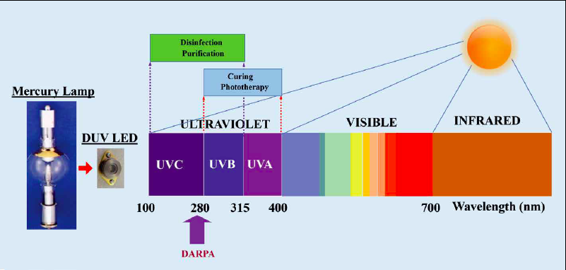
The main motivation for making LEDs with light emission below 365 nm is to create a superior mercury lamp substitute. Mercury lamp is an existing light source used in air-water purification, food disinfection and other biomedical fields. It is bulky and fragile, and requires a high working voltage. Moreover, due to the harm of mercury to food, water and biomedical industry, there is still a problem of environmental pollution. The production of high-efficiency, high-power LEDs operating in UVB and UVC is likely to generate considerable revenue, as this light source can meet a variety of critical applications (see Figure 1). Their compact structure, long life, pulse operation options, and easy integration with silicon electronic devices are conducive to their development.

Figure 1: important applications of solar spectrum and UV LED. The figure shows the wavelength requirements of various application systems.
Major milestones
The two pioneers of UV LED are our team from the University of South Carolina and the team from NTT in Japan. In early 2001, NTT reported a device that emits light at 346 nm, and soon after, we launched another led with a peak output at 341 nm. These two devices have opened up a new field, and pairing AlGaN and AlInGaN layers is their first active region feature. By the end of this year, we have made further progress to achieve 315nm emission, which is the edge of UVB field. One year later, we achieved even greater success. We reported an LED with an output power of milliwatts, emitting at 278 nm, just in the UVC band.
All of these LEDs have the same architecture. Their core is an AlGaN multiple quantum well surrounded by n-type and p-type AlGaN layers. Above the p-type side is the P + GaN layer, which supports hole injection. These LEDs are based on sapphire substrate and epitaxial AlN buffer layer with thickness of 0.1-0.2 μ m, which are formed by pulse epitaxy at medium temperature. In order to improve the quality of materials, AlGaN / AlGaN superlattices are used. Combined with dislocation filtering and strain management, these superlattices provide the basis for the growth of N + - AlGaN (n contact layer) layers with a thickness of more than 2 μ M.

Fig. 2: (a) epitaxial layer structure of the first generation device. (b) The epitaxial layer design of the second generation device can generate 1 MW power and the external quantum efficiency (EQE) is 1%. The arrows (1 to 4) describe the key design changes that result in higher power and EQE values. (c) Device configuration with flip chip geometry. (d) Transmission electron microscopy of nested short period superlattices for forming strain / defect relief AlN / AlGaN superlattices.
Like many first generation LEDs, the external quantum efficiency of these devices is very low. This can be attributed to four factors: epitaxial defects caused by lattice mismatch growth of AlN / AlGaN layers on sapphire; the low doping efficiency in p-AlGaN layers; the absorption of many photons from quantum wells by hole supplied P + - Gan; and the more serious low light extraction rate at the shortest wavelength.
By solving these problems, UV LED developers have made great progress in the next two years. For our team and several other U.S. agencies, the effort was supported by DARPA and the U.S. Army. They funded the suvos program, which was run by Lieutenant Colonel John carrano. During the suvos program, we improved our materials and growth, as well as device design and packaging. These improvements create a device with an external quantum efficiency of about 1% and an output power of nearly 1MW at a driving current of 25mA.
Better performance results from the combination of the following aspects: high temperature, migration enhanced pulse epitaxy for the growth of AlN buffer layers with a thickness of more than 2 μ m; the introduction of nested superlattices into the AlGaN layer of AlN / AlGaN superlattices; the Mg doped AlGaN electron barrier layer; the addition of polarization doped and graded p-AlGaN layers (see Fig. 2 (a) and 2 (b)); and flip chip devices on metal substrates (see Fig. 2 (c)).
As mentioned above, one of the features of our second generation devices is the improved superlattice design, which helps to compensate for defects and strain management, as well as to increase output power (Fig. 2 (d)). In this improved structure, AlN / alxga1 xn superlattices are nested short period superlattices. They are Al based on the aluminum componentxGa1-xThe superlattice is composed of nested short period alxga1 xn / allyga1 yn superlattices with average thickness. By using this method, we can grow crack free and high quality Al with thickness far over 2 μ MxGa1-xN + layer (n contact layer). This layer is integrated into our led to increase the current diffusion, alleviate the current congestion and increase the power saturation current. Thermal management has also been improved, thus extending the life of the device.
Subsequently, we have made substantial progress. By 2005, we have been able to report on the stability of our devices and their applicability in biochemical detection. We have demonstrated high-power and stable UV LEDs, laying a solid foundation for their commercialization in air and water purification applications. Although these devices are far from keeping pace with the times, they provide performance levels that are very effective in killing viruses and bacteria, such as Ecoli.
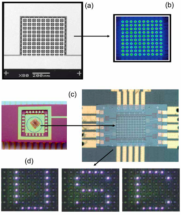
In addition to making significant contributions to the development of traditional large area UVC led, we also demonstrated a micro pixel device. The configuration reported in 2004 contributes to thermal management. Due to the decrease of the total resistance of the device, the operating temperature of the device is lower, which is a measure against current congestion and Joule heat. Another advantage of the micropixel device is that it allows individual pixel bias, making it an ideal choice for deep UV LED displays, UVC optical communications, and deep UV lithography systems (see Figure 3). For the growth of UV LED, the most common substrate is sapphire. This material is transparent, low-cost and widely available. When combined with AlN buffer layer, it provides a good foundation for UV emitter. However, two groups in the United States that produce bulk AlN substrates, crystal is and hexatech Inc., have explored the potential of this substrate for deep UV LEDs. It should be noted that other groups were not involved in this assessment due to the high cost and limited availability of AlN substrates. Although the use of self-supporting AlN has a bright future, one of the problems in mass production of materials is that impurities will be added during the growth process, which have strong absorption effect in UVC band.

Figure 3: a 10 × 10 array of micro pixel LEDs emitting at 280 nm. (a) Scanning electron microscope image of 280 nm deep UV LED with 10 × 10 micro pixel array. The diameter of each pixel is about 30 microns. (b) The image of micro pixel led under bias voltage shows uniform emission. (c) A fully packaged device mounted on a dual in-line package and an enlarged device image clearly show the electrode geometry of the pixel matrix addressing of deep UV LED. (d) By controlling the bias, 7 x 9 mode micro pixel LED can be used in UVC display, UVC communication system and deep UV lithography system.
Commercial Conquest
In the field of deep UV LED, the university research team has promoted the development. Their knowledge has moved to start-ups, driving early commercialization. Recently, some start-ups have formed partnerships or have been acquired by large companies.
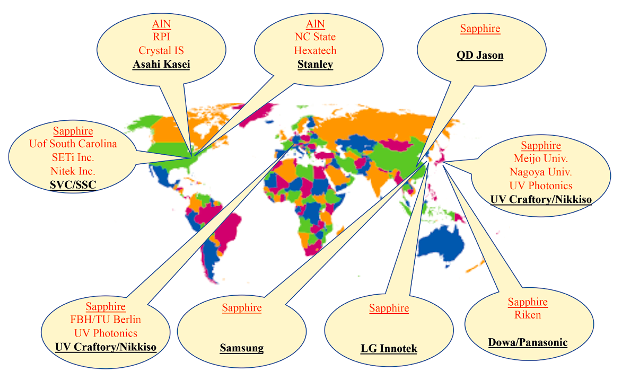
Our team started this trend. We have acquired two small businesses of semiconductor Inc., which are located in the state of Columbia, seosl Inc., and semiconductor Inc., respectively. Similarly, the technology of Nagoya University and Meiji University gave birth to UV craft, a start-up that was subsequently acquired by Nikkiso / FPG. At the same time, RIKEN's technology was directly acquired by Dowa / Panasonic; recently, the technology of Berlin Polytechnic University / FBH in Germany was transferred to UV photonics.
The development of deep UV LED based on AlN is similar. The technology invented by rensler Polytechnic laid the foundation for the establishment of crystal is, which has been acquired by Asahi Kasei. Similarly, research at North Carolina State University created hexatech, which is now part of Stanley. In addition, large companies such as Samsung, LG Innotek, QD Jason and Nichia have also started to enter the field of deep ultraviolet.

Figure 4: Global Partnership for the development of deep UV LED. In addition, the substrate materials used by each team are shown.
Today, almost all reported deep UV LEDs have most of the structures of those early devices depicted in Figure 2 (b). But they often have a key difference. In many cases, the AlN buffer layer and AlGaN short period superlattice, which provide strain management, are replaced by thick, fully relaxed AlN buffer layers, followed by AlGaN superlattices and thick n + - AlGaN contact layers. The latter can be relaxed or pseudomorphic.
Many different methods have been used to form a relaxed thick AlN buffer layer. Such buffer layers are ideal because their low dislocation density reduces the defects in the active region and improves the internal quantum efficiency of LEDs. We are growing these buffer layers by high temperature pulse epitaxy and hydride vapor phase epitaxy, and RIKEN's researchers are preparing these buffer layers by ammonia flow modulation epitaxy, and a team from the Berlin Polytechnic University is making these buffer layers by migration enhanced lateral epitaxy and sputtering AlN using off-site high-temperature annealing.
The commercial development of deep UV LED has led to the launch of emission devices between 240 nm and 300 nm. Although great progress has been made, the external quantum efficiency and electro-optic conversion efficiency of these devices are far lower than those of visible light devices. The blue LED based on InGaN achieves about 80% electro-optic conversion efficiency, while that of 266nm and 300nm deep UV LEDs is only 5% - 6%.
Although inefficient, the life of deep UV LEDs is impressive. They typically have a life span of 10000 hours and can be used for air, water purification, disinfection, polymer curing and phototherapy (see box for details).
With the shortening of emission wavelength, the external quantum efficiency of deep UV LED decreases, and the electro-optic conversion efficiency also decreases. This is partly due to the decrease of material quality and the difficulty of doping in nitride alloys with increased aluminum content. In addition, according to a team at Kansas State University, once the emission wavelength drops below 270-280 nm, the transverse magnetic polarization emission becomes more dominant due to the reordering of valence bands. As this form of light moves laterally to the C plane, it is effectively trapped in the device and hinders the extraction of photons.

Figure 5: different packaging schemes for deep UV LEDs. The figure shows (a) various to heads; (b) aluminized heads customized for better light extraction; (c) LED chips on the substrate (Web site); and (d) packages with epoxy resin and quartz dome.
Today, commercial deep UV LED packages and dimensions vary greatly. Discrete devices can be packaged with TO-39. This is not suitable for large devices, which require excellent thermal management. The chip with the SMN is installed in the SMD. Recently, devices packaged in UV transparent epoxy resin have also been introduced (see Figure 5 for images of different device packaging schemes). For everyone working in the field of deep UV LED, the biggest challenge is to improve the device performance to a value comparable to that of visible light corresponding devices. There are two major drawbacks to the device design of today's commercial products: first, the P + - Gan hole injection layer causes light loss to the p electrode and the active region waveguide. Second, the light extraction efficiency is very low.
A method of reducing the absorption of light by the P + - GaN layer and extracting / collecting more light transmitted to the p electrode includes the use of a p-AlGaN layer.
The method was developed by sensor electronic technology, rensselear Polytechnic Institute and the U.S. Army Research Laboratory; it was also developed by a Japanese team led by RIKEN, which used reflective P contactors. Both teams achieved external quantum efficiency of up to 10%.
The greater success comes from RIKEN's collaboration with Matsushita's eco solutions. They report that by combining patterned sapphire substrate with transparent p-AlGaN contact layer, the external quantum efficiency reaches 20%.
Future development direction
In general, the development of AlGaN based deep UV LED coincides with the development of InGaN based visible LED. The latter is now combined with tunnel junctions, a technology that has begun to be explored in deep UV LEDs. Researchers at Ohio State University added MBE grown n + + / P + + - Al into the active layer grown by MOCVD0.15Ga0.85The UV transparent AlGaN tunnel junction contact layer made of N can double the output power and external quantum efficiency of LED emitting in the range of 280-290nm.
Another research area is deep UV integrated optics. In this paper, we focus on integrating UVC optical and electronic components on chip with UVC transparent waveguide, which is made of AlN or aluminum rich AlGaN. In a collaboration led by researchers from Nanjing University of Posts and telecommunications, our team has provided a preliminary demonstration of integrating UVC LEDs and detectors with planar and channel waveguides (see Figure 6 (a), which details the device integration method, and Figure 6 (b) shows the image of integrated UVC LED / detector).
This success has contributed to the great development of deep UV LED in the past 20 years. With the improvement of its stability and reliability, as well as the improvement of its output power and cost advantages, its applications will surge. The development path of deep UV LED will basically follow the development path of its blue predecessors. It went faster in some stages, from its first demonstration in 2002 to the emergence of the first commercial products in five years. However, the expansion of technology, the improvement of power and efficiency took another 10 years, which are the basic elements of manufacturing low-cost devices that can provide sufficient performance. Once these new insights into device development are integrated into mass production, it will lead to an increase in the efficiency of commercial deep UV LEDs. In the past 20 years, we have come a long way. In the new 20 years, we should go further.
Application of UV LED
The applications of deep UV LED can be divided into disinfection, biomedical instruments, polymer curing and biochemical sensing.

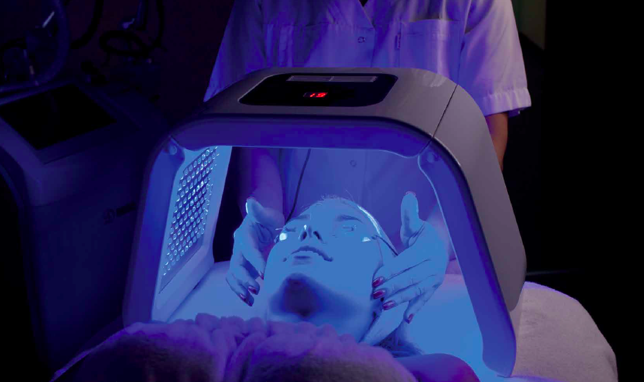
A point is used for the water purification system (left). Contains UVC LED array air conditioning system can reduce the list of viruses and bacteria (in). Psoriasis treatment system based on UVB LED (right).
Since the earth's ozone layer blocks solar radiation in UVC band, most organisms have no survival mechanism to cope with the radiation in this spectral range. When organisms are exposed to radiation, RNA / DNA will change, affecting reproduction.
As a result, organisms become inactive. Note that different organisms require different dose levels and, to some extent, wavelength selection. When the organism is exposed to UVC led with output power of 100-125 MW and peak wavelength of 265 nm, 40-50 MJ / cm2 The flux can render most bacteria, spores, and viruses inactive. Some UVC LED companies or their strategic partners are selling purification systems based on UVC LED, which can be used in medium capacity point water purification.
Recently, some companies have begun to study the use of ultraviolet radiation for surface purification of viruses, such as covid-19. Led by the Seoul viosys company. The company's violet deep UV LED technology is being used in the fresh air brand produced by Gree Electric, China's largest air conditioner manufacturer. Another adoption of this technology is RGF environment group, a leading supplier of indoor air treatment in the United States. These efforts show that deep UV LED technology can provide protection against a variety of pests.
Another type of deep UV LED application is polymer curing. When UVA / B / C radiation reaches the polymer, a chemical reaction is initiated. What happens is that exposure to photoinitiator molecules produces free radicals, which promote the polymerization of monomer and oligomer molecules. Curing applications are the backbone of key industries such as coatings, ink printing, adhesives and lithography.
Deep UV LED is also very effective in producing photochemical reactions in organisms. LEDs emitted in UVB are an excellent source for enhancing metabolite concentrations. This means that the growth cycle, flavor and quality of plants can be controlled by deep UV irradiation. In addition to bringing economic benefits, this also makes these ultraviolet light sources have far-reaching significance in dealing with global food shortage.
Phototherapy systems offer another business opportunity for deep UV LEDs. These systems are currently being used to treat vitamin D deficiency, seasonal mood disorders and psoriasis.
Professor Chen Changqing, chairman of the board of deep violet technology, was invited to give the conference report "semiconductor UV LED and its application
Company News, December 29, 2017, 870 views
The source of wisdom and life -- the application of deep UV in water purifier
Technology sharing · May 27, 2021 · 201 views
Good News | Warmly Celebrating Our Company's Dr. Chen Jingwen's Selection into the "China Optics Valley 3551 Talent Plan"
Company News, June 28th, 141 views
Water related approval approved, and Youweixin has obtained authoritative certification in the field of drinking water hygiene and safety
Company News, September 24th, viewed 97 times
Youweixin has won the first prize in the Wuhan Science and Technology Innovation Competition!
Company News, January 15th, 33 views
[video tutorial] deep design of deep UV uvc-led sterilization scheme
Technology sharing · February 11, 2020 · 1410 views
Is 230nm UVLED light harmless to human body? The German research team has used it against hospitals
Industry Information · June 14, 2020 · 524 views
Three questions lead you to understand the market of ultra violet uvc-led
Technology sharing · October 20, 2018 · 828 views
