Experts say: DUVTek announced deep ultraviolet LED high performance chip
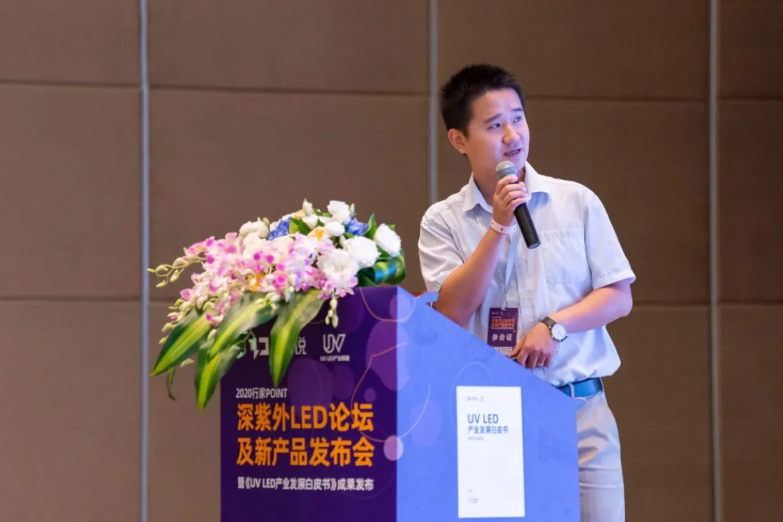
On July 3, at the "2020 expert point · deep UV LED forum and new product release conference and" white paper on UV LED industry development "held in Shenzhen, Hubei Shenzi shared the keynote speech of high performance chip. Dr Leung said that at present, there are challenges in the epitaxy, chip and package of deep UV LED, but the most difficult is in epitaxy. The main difficulties are the growth process and devices. Therefore, how to prepare high epitaxial quality materials, high light extraction efficiency structure, high reliability UV LED devices become the bottleneck of the industry development.

So, in the epitaxial chip technology, what are the technical highlights of DUVTek?
1. Preparation of high quality AlN substrate
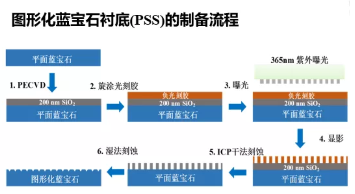
For deep violet epitaxial growth, a patterned sapphire substrate process is adopted, which is self-designed and fabricated on planar sapphire substrate. The preparation process first uses PECVD to deposit 200 nm SiO 2 mask, and then carries out photolithography, ICP etching and wet etching in turn.
Based on the above substrates, AlN materials were grown by MOCVD in three steps: low temperature AlN nucleation, pulse atomic layer deposition and high temperature AlN continuous growth. The surface of AlN film is smooth and crack free, which lays a good foundation for high performance devices.

Source: 2020 expert point deep UV forum and new product launch - DUVTek speech ppt
2. Growth process of deep ultraviolet LED material with electronic retarder
The electron migration ability of AlGaN is greater than that of AlGaN. In order to balance the migration ability of electrons and holes, Hubei deep violet added a layer of superlattice electron retarder structure before AlGaN expansion layer to suppress electron overflow.
It has been revealed that DUVTek has designed three kinds of structures: one is the structure with uniform al component, the other is the structure with lower Al component, and the other is the structure with higher Al component. The influence of three structures on device performance is studied.
The results show that the crystal quality of the four samples is the same, excluding the influence of crystal quality on device performance, the interface of quantum well and superlattice electronic reducer is steep.
3. Design and technology of high efficiency deep ultraviolet LED device invisible cutting technology
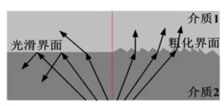
The substrate technology used in Hubei deep violet is to form fully roughened side wall by using multi laser invisible cutting technology in the equivalent coarsening area, so as to alleviate the total reflection of TM mode ultraviolet light on sapphire side wall, so as to improve the light extraction efficiency. It is revealed that under this cutting process, the optical power of four roughening knives is increased by 19.62% compared with one knife at 100mA.

Source: expert point deep UV forum and new product launch in 2020
In addition, in the design and technology of microlens array, the output power of deep UV LED can be increased by 26.7% by using moth eye nano film.
In addition to sharing technology highlights, DUVTek also released a deep UV LED chip.
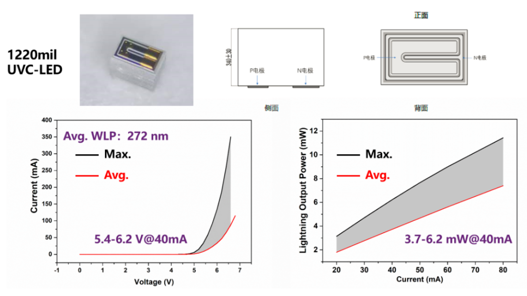
Dr. Liang Renzhe showed the 1220mil deep UV LED chip of DUVTek at the conference, and the mainstream chip realized by the combination of the above technologies. The chip can realize 3.7-6 2mW@40mA , 9-15mW@100mA The peak wavelength of 272nm is 272 nm, and the output wavelength of WPE is 2.41%.

Source: expert point deep UV forum and new product launch in 2020
In his speech, Dr. Liang Renzhe revealed that next, Hubei dark violet will continue to work in the direction of shorter wavelength and higher power (high light efficiency) to provide more cost-effective deep UV LED chips.
Zhang Hao: evaluation and application of UVA led photocatalysis technology for air sterilization and disinfection
Industry News · February 15, 2020 · 1843 views
Good News | Warmly Celebrating Our Company's Dr. Chen Jingwen's Selection into the "China Optics Valley 3551 Talent Plan"
Company News · June 28, 2023 · 576 views
High power, high light intensity! DUVTek over flow water sterilization uvc-led has been mass produced
Company News · May 17, 2021 · 622 views
Biological safety of 222 nm lamp for sterilization
Industry News · December 19, 2020 · 2477 views
Sohu.com reports: Shenzhen purple technology shines on the scene of 2018 Wuhan light Expo
Media Report · November 9, 2018 · 518 views
Breakthrough in UV LED Technology: Wuhan Youweixin Builds a New Ecological Environment for Healthy Sterilization Industry, Leveraging Global Momentum ..
Company News · April 27th · 75 views
It does not destroy the nutrition and flavor. UVC ultraviolet is perfect for juice sterilization
Technical Sharing · November 3, 2018 · 1104 views
Virus without lover's affection, DUVTek actively assists Wuhan Tongji Hospital
Company News · February 26, 2020 · 748 views
